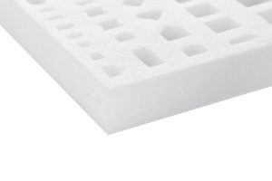
Shrinking electronics are creating a packaging challenge that is easy to underestimate: the smaller the device becomes, the less room there is for unwanted movement, pressure, and electrostatic exposure. Compact circuit assemblies, optical modules, sensors, and power components often contain delicate features within increasingly tight housings.
As a result, custom packaging foam is shifting from general cushioning toward application-specific engineering. At Proflexpack, we approach this change from the perspective of product geometry, material behavior, handling conditions, and the practical demands of international electronics logistics.
Greater Precision In Packaging Geometry
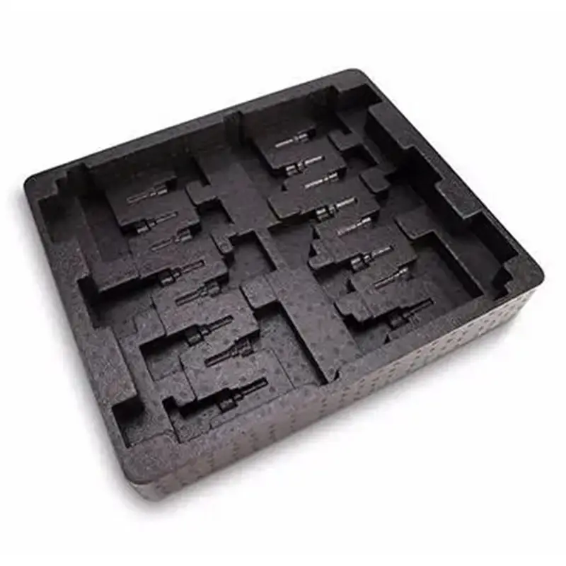
Miniaturized products rarely have simple rectangular profiles. Connectors may extend from narrow housings, optical components require controlled clearances, and circuit assemblies can contain fragile protrusions at several locations. Packaging cavities must account for these differences rather than relying on uniform surrounding material. Precise cavity dimensions help distribute contact across suitable structural areas while keeping sensitive surfaces away from unnecessary pressure.
Three-dimensional CAD has become particularly useful in this environment. Engineers can map product contours, mounting points, cable exits, and clearance zones before a physical prototype is produced. Such digital coordination is valuable for Semiconductor Discrete Devices, Computer Motherboards, Sensors, and New Power Electronic Components, where even relatively small dimensional errors may affect how an assembly sits inside its protective cavity.
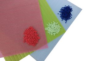
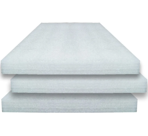
Material geometry matters just as much as dimensional accuracy. EPP foam allows packaging designers to create shaped cavities, channels, recesses, and support zones around individual components. Instead of treating cushioning as one continuous mass, engineers can place structural support where impact forces are most likely to reach the product.
Lightweight Protection With Targeted Support
Weight reduction has become an important consideration as electronics move through air, ocean, express, and multimodal logistics networks. Excess packaging adds handling requirements and shipping mass, yet reducing material indiscriminately may leave vulnerable areas insufficiently supported. The more useful approach is selective reinforcement, with cushioning concentrated around impact-sensitive regions and unnecessary material reduced elsewhere.
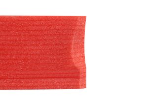
Material resilience also affects packaging performance. EPP has a cellular structure that combines low weight with energy-absorption characteristics, making it suitable for products that encounter repeated handling. EPP foam may be incorporated into reusable transport concepts for equipment such as Optical, Measuring, and Testing Instruments, Power Supplies, Portable Computers, and compact industrial electronics.
The physical behavior of the protected product should guide the design rather than material preference alone. A rigid optical assembly, for example, may require different support points from a lightweight remote control. Similar distinctions apply to Power Adapters, Smart Remote Controls, Wires and Cable Assemblies, and Electronic Heating Components, each of which presents its own combination of mass, shape, and sensitivity.
ESD Awareness Becomes More Integrated
Electrostatic discharge deserves greater attention as functional density rises. A compact electronic assembly may contain numerous sensitive components within a limited footprint, increasing the importance of controlling how packaging materials interact with the product during packing, unpacking, and transportation. Packaging decisions should be considered alongside grounding procedures, handling protocols, and storage conditions.
For ESD-sensitive applications, custom packaging foam may incorporate suitable anti-static material characteristics alongside physical cushioning. The packaging system should be assessed as a whole rather than treating electrostatic protection as an isolated material specification. Surface properties, product contact areas, operator handling, and the surrounding packaging environment all influence practical performance.
This consideration extends across several electronics categories. Active and Passive Components, Optoelectronic Materials, Single-Mode Fiber Optic Equipment, and Data Communication Multimedia Systems may require controlled packaging environments because their functional elements can be sensitive to electrostatic events. Proper packaging architecture helps reduce unnecessary movement while supporting established ESD handling procedures.
Digital Engineering Accelerates Design Decisions
Packaging development increasingly relies on digital product information rather than physical trial and error alone. CAD files provide reference geometry for cavity development, while prototypes allow engineers to examine fit, insertion force, access points, and potential contact issues. This combination shortens the distance between product engineering and packaging engineering.
At Proflexpack, we use 3D/CAD development and a 72-hour rapid prototyping process to evaluate packaging concepts against actual product geometry. Our EPP-based insert program includes ITEM 3110728 and MFG 0728B, with firm structural support, high-stability shock absorption, and drop and vibration testing used during development. Such methods are relevant to electronics and precision equipment where predictable fit matters across production quantities.
Digital workflows are also useful when a product family contains several related configurations. Computer Chassis, Microcomputers, Multimedia Computers and Servers, and Optoelectronic Equipment may share similar platforms while differing in dimensions, connectors, or external features. Parameter-based design makes these variations easier to accommodate without rebuilding the entire packaging concept from the beginning.
Conclusion
Electronics miniaturization is changing protective packaging at several levels simultaneously: geometry is becoming more precise, cushioning is becoming more selectively distributed, ESD considerations are moving closer to the core design process, reusable systems are gaining practical value, and digital engineering is making iteration more efficient.
Proflexpack applies these principles through a first-person engineering approach, combining material knowledge, CAD development, prototyping, and testing to address demanding electronics and industrial applications. As devices continue to pack greater functionality into smaller footprints, custom packaging foam and carefully engineered EPP foam designs will increasingly function as integral parts of the product logistics strategy rather than simple protective accessories.