-re0ekjsqlb4ojigkuutt3usg360zqvvu56lxdec0lc.png "所有proflexpacks改为proflexpack的(logo)")
The semiconductor industry, renowned for its sensitive and high-value products, necessitates stringent packaging solutions to ensure the integrity of wafers during transit. Electrostatic discharge (ESD) can severely damage semiconductor wafers, making the choice of packaging foam a critical aspect of compliance and safety. Various options exist in the market, with anti-static EPS foam inserts leading the way in providing reliable ESD safe packaging. Here, we explore three top packaging foam options for semiconductor wafers, focusing on their benefits and applications.
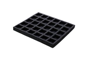
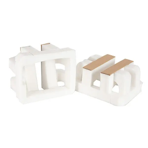
- Anti-Static EPS Foam Inserts
Anti-static EPS foam inserts are engineered to offer stable static control while providing firm protection for semiconductor wafers. These high-compression strength inserts feature a rigid structure that ensures excellent load distribution and resistance to deformation. This capability makes them particularly suitable for packaging large electronics and precision equipment that require robust shock absorption during shipping.
One significant advantage of anti-static EPS foam inserts is their ability to maintain stability even during long-distance transport. The bead-fused cellular structure efficiently manages shock and energy, effectively dispersing impact forces. This feature is crucial for wafers, which can easily crack or suffer damage from even minor impacts.
With their inherent ESD-safe properties, these inserts are ideal for ensuring compliance with industry standards, reducing the risk of electrostatic discharge and enhancing the overall security of semiconductor packaging.
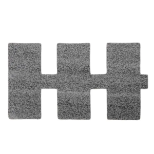
- ESD Safe Polyurethane Foam
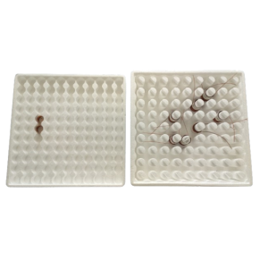
Polyurethane foam is a flexible option that adapts well to various shapes and sizes, making it a reliable choice for semiconductor wafers. ESD safe polyurethane foam is designed with specific conductive additives that help dissipate static electricity. This quality provides an additional layer of protection against ESD while maintaining effective shock absorption.
To optimize transport space, polyurethane foam can be precisely custom-cut or molded to cradle any wafer configuration. Its lightweight nature further reduces shipping costs while ensuring that wafers remain protected from vibrations and shocks.
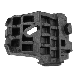
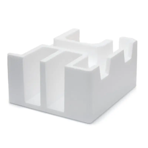
- ESD Safe Custom Foam Solutions
For companies requiring tailored solutions, ESD safe custom foam options are available that cater specifically to the unique needs of semiconductor manufacturers. These solutions combine various foam materials, including anti-static EPS and polyurethane foams, to create bespoke packaging that meets precise specifications.
By employing specialized design techniques, manufacturers can achieve optimal performance in both static control and cushioning. Custom solutions also allow for enhanced branding opportunities through unique shapes or colors, appealing to companies looking to strengthen their market identity.
Elevating Semiconductor Safety with ProFlexPack
When selecting ESD safe packaging foam for semiconductor wafers, it’s crucial to consider the specific requirements of your products. At ProFlexPack, we specialize in providing high-quality anti-static EPS foam inserts designed to deliver unparalleled protection and stability. Our commitment to excellence ensures that your valuable semiconductor wafers are packaged securely, compliant with industry standards, and protected against ESD risks.
Partnering with ProFlexPack means integrating innovative packaging solutions into your supply chain, enhancing the safety and reliability of your semiconductor products. We invite you to explore our offerings and see how we can help you elevate your packaging strategies for optimal performance and compliance.